ADM7154

RECOMMENDED FOR NEW DESIGNS

600 mA, Ultralow Noise, High PSRR, RF Linear Regulator

Part Models
12
1ku List Price
Starting From $2.75
Viewing:

Part Details

  • Input voltage range: 2.3 V to 5.5 V
  • Maximum load current: 600 mA
  • Low noise
    • 0.9 µV rms total integrated noise from 100 Hz to 100 kHz
    • 1.6 µV rms total integrated noise from 10 Hz to 100 kHz
  • Noise spectral density: 1.5 nV/√Hz from 10 kHz to 1 MHz
  • PSRR of 90 dB from 200 Hz to 200 kHz; 58 dB at 1 MHz, VOUT = 3.3 V, VIN = 3.8 V
  • Dropout voltage: 120 mV typical at VOUT = 3.3 V, IOUT = 600 mA
  • Initial accuracy: ±0.5%
  • Accuracy over line, load, and temperature: −2.0%(minimum),
  • +1.5% (maximum), from −40°C to +85°C
  • Quiescent current, IGND = 4 mA at no load
  • Low shutdown current: 0.2 μA
  • Stable with a 10 µF ceramic output capacitor
  • Adjustable and fixed output voltage options: 1.2 V, 1.8 V, 2.5 V, 2.8 V, 3.0 V, 3.3 V (16 standard voltages between 1.2 V and 3.3 V available)
  • 8-lead LFCSP and 8-lead SOIC packages
  • Precision enable

ADM7154
600 mA, Ultralow Noise, High PSRR, RF Linear Regulator
ADM7154 Typical Application Circuit Diagram ADM7154 Pin Diagram ADM7154 Pin Diagram
Add to myAnalog

Add product to the Products section of myAnalog (to receive notifications), to an existing project or to a new project.

Create New Project
Ask a Question

Documentation

Learn More
Add to myAnalog

Add product to the Products section of myAnalog (to receive notifications), to an existing project or to a new project.

Create New Project

Hardware Ecosystem

Parts Product Life Cycle Description
ADM7155 RECOMMENDED FOR NEW DESIGNS 600 mA, Ultralow Noise, High PSRR, RF Linear Regulator
Modal heading
Add to myAnalog

Add product to the Products section of myAnalog (to receive notifications), to an existing project or to a new project.

Create New Project

Tools & Simulations

LTspice 1


Models for the following parts are available in LTspice:

  • ADM7154-1.2
  • ADM7154-1.8
  • ADM7154-2.5
  • ADM7154-3.0
  • ADM7154-3.3

ADI Linear Regulator Design Tool and Parametric Search

Microsoft Excel download tool from ADIsimPower to generate a power supply design complete with a schematic, bill of materials, and performance specifications.

Open Tool
LTspice

LTspice® is a powerful, fast and free simulation software, schematic capture and waveform viewer with enhancements and models for improving the simulation of analog circuits.


Evaluation Kits

eval board
AD-SYNCHRONA14-EBZ

Multichannel System Clocking Device

Features and Benefits

Processing System

  • Raspberry Pi 4, ARM Cortex-A72, 2GB SDRAM

User Interfaces

  • Gigabit Ethernet
  • 2 × USB 3.0 ports
  • 2 × USB 2.0 ports
  • SPI interface
  • GPIO
  • 2 bicolor LEDs
  • Male pin header

Clock Processing Devices

  • HMC7044 (High Performance, 3.2 GHz, 14-Output Jitter Attenuator)
  • AD9545 (1 PPS Synchronizer and Adaptive Clock Translator)

Clock Outputs

  • 4 x TWINAX LVPECL AC&DC coupled, 100Ω diff
  • 2 x SMA LVPECL AC coupled*
  • 4 x SMA CMOS*
  • 4 x SMA LVDS AC coupled*

*Configurable differential outputs, 50Ω diff

Clock Inputs

  • 3 differential 100Ω SMA clock inputs
  • PPS input
  • SYNC input
  • 10MHz input

Internal references

  • 100Mhz and 122.88Mhz Ultra-Low Phase Noise VCXO's (-165dBc/Hz)
  • 40Mhz and 38.4Mhz TCXO's (±1ppm) 50MHz OCXO(+/- 10ppb)
  • Internal references are software configurable

Power supply

  • DC 12V, 3A barrel jack

Product Details

The AD-SYNCHRONA14-EBZ is an ideal self-contained device to use in evaluation and prototyping of applications that need a highly accurate frequency and phase-controlled source clock. It is designed around the Analog Devices AD9545 and HMC7044 and greatly simplifies clock distribution and multi-channel synchronization in complex systems. It is intended to be used by trained professionals in a laboratory environment, and not intended as an end product for commercial use. It can be taken as a complete reference design and customised as required for any end customer applications. Full design details are made available free of charge.

The AD-SYNCHRONA14-EBZ comes in a 1U mechanical form factor. Using popular industry connector SMA and TwinAX interfaces most labs will already have the needed cables.

With its internal OCXO it can operate in standalone mode or be fed from a choice of external sources, such as 3 separate high speed differential clock inputs, a 10MHz reference and 1PPS. This flexibility combined with the capability to select either of the internal VCXO options of 100MHz or 122.88MHz, gives almost unlimited choice for the frequency of interest and accuracy needed for a wide variety of application areas. 

APPLICATIONS

  • High accuracy reference clock distribution
  • Systems clocked from a single source
  • Clocks derived from 100MHz or 122.88MHz
  • Phased Array Systems, RADAR, EW, SATCOMS, SDR
  • Bench Equipment
  • Remote controlled operation

eval board
AD-GMSL2ETH-SL

FPGA-based 8x GMSL to 10 Gb Ethernet Adapter

Features and Benefits

  • Edge compute platform for machine vision and real-time sensor fusion for autonomous robots and vehicles applications
  • 8 x GMSL2 camera interfaces with up to 6 Gbps/channel
  • 10 Gbps SFP+ Ethernet interface
  • IEEE 1588 Precision Time Protocol for synchronization with host systems and other edge devices
  • Advanced embedded processing capabilities
  • ROS2 compliant
  • Advanced camera triggering functions and control features
  • Open-source software stack and FPGA design to enable custom applications development

Product Details

The AD-GMSL2ETH-SL is an edge compute platform enabling low-latency data transfer from eight Gigabit Multimedia Serial Link™ (GMSL) interfaces on to a 10 Gb Ethernet link. The target applications include autonomous robots and vehicles where machine vision and real-time sensor fusion is critical.

The system includes two MAX96724 Quad Tunneling GMSL2/1 to CSI-2 Deserializers, enabling connectivity to eight GMSL cameras. The video data from the cameras is transferred from the MAX96724 deserializers via MIPI CSI2 interfaces to an AMD KV26 System on Module which implements the logic to aggregate the video data from all the GMSL cameras into a 10 Gb Ethernet link, so that it can be sent to a central processing unit.

The IEEE 1588 Precision Time Protocol (PTP) with hardware timestamping is supported, enabling accurate synchronization with host systems and other edge devices. The AD9545 Quad Input, 10-Output, Dual DPLL/IEEE 1588, 1 pps Synchronizer and Jitter Cleaner is used to generate the required clocks for the 10 Gb Ethernet interface and the PTP logic.

A software networking stack can be used to realize the communication over the 10 Gb Ethernet link. Since the system runs Linux tools like gstreamer can be used to send the video data to a host and remote connection into the system is possible via ssh. The software network stack has limitations in terms of the maximum achievable transfer rate, and for this reason there is also the option to have an FPGA accelerated UDP or TCP implementation with Real Time Transfer (RTP) protocol for data packetization, which can get up to the maximum achievable data rate on the 10 Gb ethernet interface.

Accurate camera triggering control is achieved through dedicated FPGA logic, with configurable frequency and phase as well as selecting the trigger source between the internal logic and external signals.

Sixteen (16) general purpose I/O pins are available with software configurable functionality, operating at 3.3 V voltage level. A RS232 dedicated interface can be used to connect UART peripherals such as GNSS devices.

The design is accompanied by an open-source software stack and FPGA design, and reference applications, enabling custom software development to start from a proven implementation.

APPLICATIONS

  • Autonomous robots and vehicles

eval board
EVAL-ADM7154

ADM7154 Evaluation Board

Features and Benefits

  • Input voltage range: 2.3 V to 5.5 V
  • Maximum output current: 600 mA
  • Low noise
  • 0.9 µV rms total integrated noise from 100 Hz to 100 kHz
  • 1.6 µV rms total integrated noise from 10 Hz to 100 kHz
  • Initial accuracy: ±0.5%
  • Fixed 3.3 V (ADM7154) and adjustable (ADM7155) output versions
  • 8-lead LFCSP and 8-lead SOIC packages

Product Details

The ADM7154CP-3.3EVALZ, ADM7154CP-1.8EVALZ and ADM7155CP-02-EVALZ evaluation boards are used to demonstrate the functionality of the ADM7154 and ADM7155 linear regulators, respectively.

Simple device measurements, such as line and load regulation, dropout, and ground current, can be demonstrated with just a single voltage source, a voltmeter, an ammeter, and load resistors.

For more details about the linear regulators, refer to the ADM7154 and ADM7155 data sheets.

Evaluation Kit Contents
  •     ADM7154CP-3.3EVALZ, ADM7154CP-1.8EVALZ or ADM7155CP-02-EVALZ evaluation board
Additional Equipment Needed
  •     DC power supply
  •     Multimeters for voltage and current measurements
  •     Electronic or resistive loads

eval board
AD-FMCADC4-EBZ

ADA4961 & AD9680 Analog Signal Chain Evaluation and AD9528 Converter Synchronization

Features and Benefits

  • Four channels of 1.0 GSPS conversion utilizing JESD204B high speed serial interface
  • Driver amplifier interface with 21dB voltage gain adjustment
  • Optional on-board or external clocking
  • Specific design and I/O added for multi-board synchronization

Product Details

The AD-FMCADC4-EBZ is a high speed 4-channel data acquisition board featuring two AD9680 dual channel ADC at 1000 MSPS and four ADA4961 low distortion, 3.2 GHz, RF DGA driving each converter. The FMC form factor supports the JESD204B high speed serial interface. All clocking and channel synchronization is support on-board using the AD9528 clock generator. This product is designed for sampling wide bandwidth analog signals up to the second Nyquist zone. The combination of wide input bandwidth, high sampling rate, and excellent linearity of the AD9680 is ideally suited for spectrum analyzers, data acquisition systems, and a wide assortment of military electronics applications, such as radar and jamming/anti-jamming measures.


The board meets most of the FMC specifications in terms of mechanical size, mounting hole locations, and more. Although this board does meet most of the FMC specifications, it’s not meant as a commercial off the shelf (COTS) board. If you want a commercial, ready to integrate product, please refer to one of the many FMC manufacturers and the FMC specification (ANSI/VITA 57.1).

This board is targeted to use the ADI reference designs that work with Xilinx development systems. ADI provides complete source (HDL and software) to re-create those projects (minus the IP provided by the FPGA vendors, which we use), but may not provide enough info to port this to your custom platform.

The design of the board is specifically tailored to synchronizing multiple AD-FMCADC4-EBZ boards together. For more information on synchronization please refer to A Test Method for Synchronizing Multiple GSPS Converters. The reference design includes the device data capture via the JESD204B serial interface and the SPI interface. The samples are written to the external DDR-DRAM. It allows programming the device and monitoring its internal registers via SPI.

eval board
AD-FREQCVT1-EBZ

TX/RX channels, Frequency conversion from 1‑100 MHz up to 400 MHz

Product Details

The AD-FREQCVT1-EBZ is an add on board for the FMCOMMS3/4/5 boards which contain the AD9361. While the complete chip level design package can be found on the ADI product pages, information on the card, how to use it, the design package that surrounds it, and the software which can make it work, can be found on the analog wiki site.

The purpose of the AD-FREQCVT1-EBZ is frequency up or down conversion to allow the AD9361 to operate down to 1MHz.

eval board
AD-FMCOMMS11-EBZ

Direct RF to Baseband Transmit Radio

Features and Benefits

  • TX
    • 16-bit 12GSPS RFDAC
    • JESD204B Interface
      • 8 lanes up to 12.5Gbps
    • 1x/2x/4x/6x/8x/12x/16x/24x/32x Interpolation
    • 64-bit NCO at max rate
    • Analog Modes of Operation:
      • Normal Mode: 6GSPS DAC rate
        • Synthesis up to 2.5GHz (1st Nyquist)
      • Mix Mode: 6GSPS DAC rate
        • Synthesis in 2nd & 3rd Nyquist zones
      • 2X Normal Mode: 12GSPS DAC rate
        • Synthesis up to 6GHz (1st Nyquist)
      • Excellent dynamic performance
  • RX
    • 3.2GHz full power bandwidth at 2.5GSPS
      • Noise Density = -149.5dBFs/Hz, ENOB = 9.5 bits
      • SFDR = 77 dBc at 1GHz Ain (2.5Gsps)
      • SFDR = 77dBc at 1.8GHz Ain (2.5Gsps)
    • +/-0.3 LSB DNL, +/-1.0 LSB INL
    • Dual supplies : 1.3V and 2.5V
    • 8 or 6 Lane JESD204B Outputs
    • Programmable clipping threshold for Fast Detect output
    • Two Integrated wide band digital down converters (DDC) per channel
      • 10-bit complex NCO
      • 2 cascaded half band filters (dec/8, dec/16)
    • Timestamp for synchronous processing alignment
      • SYSREF Setup/Hold detector
    • Programmable Interrupt (IRQ) event monitor

Product Details

The AD-FMComms11-EBZ board is a system platform board for communication infrastructure applications that demonstrates the Direct to RF (DRF) transmitter and observation receiver architecture. Using high sample rate RFDAC(s) and RFADC(s), a number of components in previous generation transmitters can be eliminated, such as mixers, modulators, IF amplifiers and filters. The objective being to bring the ADC or DAC as close to the antenna as possible, leading to possibly more cost effective and efficient communications solution.

It is composed of multi-GSPS RF ADC and DAC, AD9625 and AD9162 respectively. The transmit path contains a balun, low pass filter, gain block and variable attenuation to produce an output appropriate for a power amplifier module. Along the observation path, the PA output is coupled back into the board through a variable attenuator, a balun and finally the ADC. Clock management is taken care of on board; all the necessary clocks are generated from a reference. Power management is present as well.

AD-SYNCHRONA14-EBZ
Multichannel System Clocking Device
AD-SYNCHRONA14-EBZ Evaluation Board - Front View AD-SYNCHRONA14-EBZ Evaluation Board Evaluation Board - Back View AD-SYNCHRONA14-EBZ Evaluation Board
AD-GMSL2ETH-SL
FPGA-based 8x GMSL to 10 Gb Ethernet Adapter
AD-GMSL2ETH-SL Board Photo Angle View AD-GMSL2ETH-SL Board Photo Top View AD-GMSL2ETH-SL Board Photo Bottom View AD-GMSL2ETH-SL Block Diagram
EVAL-ADM7154
ADM7154 Evaluation Board
Eval_AD715x Eval-ADM7154PFCSP
AD-FMCADC4-EBZ
ADA4961 & AD9680 Analog Signal Chain Evaluation and AD9528 Converter Synchronization
AD-FMCADC4-EBZ Evaluation Board (top) AD-FMCADC4-EBZ Evaluation Board (bottom)
AD-FREQCVT1-EBZ
TX/RX channels, Frequency conversion from 1‑100 MHz up to 400 MHz
AD-FREQCVTI-EBZ Board AD-FREQCVTI-EBZ Block Diagram
AD-FMCOMMS11-EBZ
Direct RF to Baseband Transmit Radio
AD-FMCOMMS11-EBZ Block Diagram AD-FMCOMMS11-EBZ Evaluation Board AD-FMCOMMS11-EBZ Evaluation Board - Top View AD-FMCOMMS11-EBZ Evaluation Board - Bottom View

Reference Designs

Figure 1. CN0511 Functional Block Diagram
CN0511 Circuits from the lab

DC to 5.5 GHz Signal Generator with +/-0.5 dB Calibrated Output Power

Features and Benefits

  • DC to 5.5 GHz Single Tone Generator
  • +/- 0.5 dB  Wideband Amplitude Calibration from 0 dBm to -40 dBm
  • 48-Bit Frequency Tuning Resolution (~43 uHz)
  • Onboard VCXO for Quick Bring Up
  • Compatible with Raspberry Pi 3B+, 4, Zero W, Zero 2W
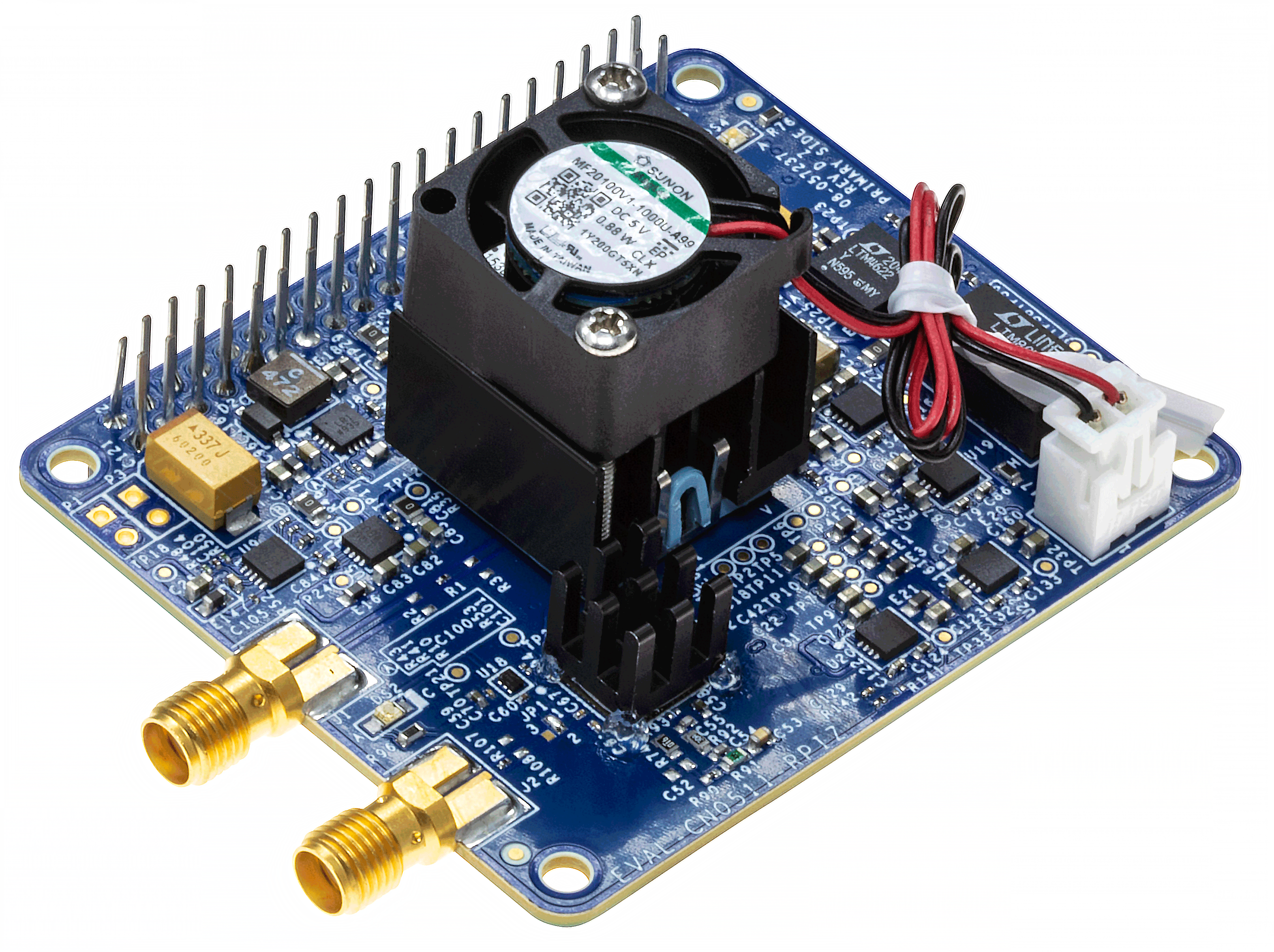
CN0511
DC to 5.5 GHz Signal Generator with +/-0.5 dB Calibrated Output Power
Figure 1. CN0511 Functional Block Diagram
EVAL-CN0511-RPIZ Evaluation Board
EVAL-CN0511-RPIZ Evaluation Board - Top View
EVAL-CN0511-RPIZ Evaluation Board - Bottom View

Latest Discussions

Recently Viewed