CN0185


Overview
Design Resources
Design & Integration File
- Schematic
- Bill of Materials
- Gerber Files
- PADS Files
- Assembly Drawing
Evaluation Hardware
Part Numbers with "Z" indicate RoHS Compliance. Boards checked are needed to evaluate this circuit.
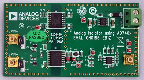
- EVAL-CN0185-EB1Z ($58.85) A Novel Analog-to-Analog Isolator Using an Isolated Sigma-Delta Modulator, Isolated DC-to-DC Converter, and Active Filter
Device Drivers
Software such as C code and/or FPGA code, used to communicate with component's digital interface.
Features & Benefits
- Analog to analog isolation
- Provides both signal and power isolation
Product Categories
Markets and Technologies
Parts Used
Documentation & Resources
-
CN0185 Software User Guide10/18/2018WIKI
-
MT-101: Decoupling Techniques2/14/2015PDF954 kB
-
MT-023: ADC Architectures IV: Sigma-Delta ADC Advanced Concepts and Applications2/14/2015PDF936 kB
-
MT-022: ADC Architectures III: Sigma-Delta ADC Basics2/14/2015PDF289 kB
-
MT-031: Grounding Data Converters and Solving the Mystery of "AGND" and "DGND"3/20/2009PDF144 kB
Circuit Function & Benefits
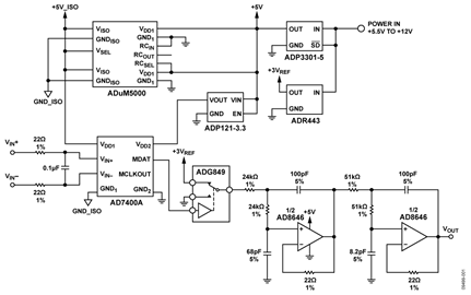
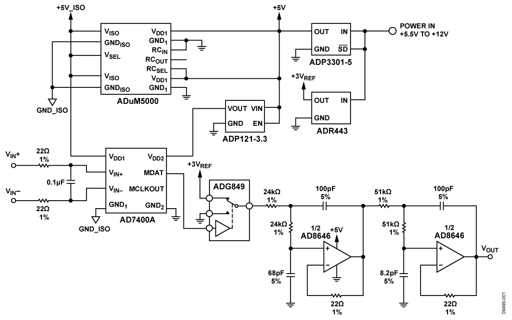
The circuit shown in Figure 1 is a complete low cost implementation of an analog-to-analog isolator. The circuit provides isolation of 2500 V rms (1 minute per UL 1577).
The circuit is based on the AD7400A, a second-order, sigma-delta (Σ-Δ) modulator with a digitally isolated 1-bit data stream output. The isolated analog signal is recovered with a fourth-order active filter based on the dual, low noise, rail-to-rail AD8646 op amp. With the ADuM5000 as the power supply for the isolated side, the two sides are completely isolated and use only one power supply for the system. The circuit has 0.05% linearity and benefits from the noise shaping provided by the modulator of the AD7400A and the analog filter. The applications of the circuit include motor control and shunt current monitoring, and the circuit is also a good alternative to isolation systems based on optoisolators.

Circuit Description
A block diagram of the circuit is shown in Figure 1. The analog input is sampled at 10 MSPS by the AD7400A Σ-Δ modulator. The 22 Ω resistors and 0.1 μF capacitor form a differential input noise reduction filter with a cutoff frequency of 145 kHz. The output of the AD7400A is an isolated 1-bit data stream. The quantization noise is shaped by a second-order Σ-Δ modulator, which shifts the noise to the higher frequencies (see the MT-022 Tutorial).
To reconstruct the analog input signal, follow the data stream by an ADG849 switch connected to a 3 V ADR443 reference to stabilize the peak-to-peak output of the MDAT.
The signal is then filtered by an active filter whose order is higher than the order of the modulator. A fourth-order Chebyshev filter is used for better noise attenuation. Compared to other filter responses (Butterworth or Bessel), the response of the Chebyshev provides the steepest roll-off for a given filter order. The filter is implemented using the dual AD8646, a rail-to-rail, input and output, low noise, single-supply op amp.
The ADuM5000 is an isolated dc-to-dc converter based on Analog Devices, Inc., iCoupler® technology. It is used for the power supply to the isolated side of the circuit containing the AD7400A. The isoPower® technology of the ADuM5000 uses high frequency switching elements to transfer power through a chip-scale transformer.
The circuit must be constructed on a multilayer printed circuit board (PCB) with a large area ground plane. Proper layout, grounding, and decoupling techniques must be used to achieve optimum performance (see the MT-031 Tutorial, Grounding Data Converters and Solving the Mystery of "AGND" and "DGND," the MT-101 Tutorial, Decoupling Techniques, and the ADuC7060/ADuC7061 evaluation board layout). Ensure that the PCB layout meets the emissions standards and isolation requirements between the two isolated sides (see the AN-0971 Application Note).
In order not to overdrive the AD8646, the input signal must be lower than the power supply (5 V). The output of the AD7400A is a stream of 1s and 0s with an amplitude equal to the AD7400A VDD2 supply voltage. Therefore, the VDD2 digital supply is 3.3 V supplied by the ADP121 linear regulator. Alternatively, if a 5 V supply is used for VDD2, attenuate the digital output signal before connecting to the active filter. In either case, well regulate the supply because the final analog output is directly proportional to VDD2.
The 5 V supply for the circuit in Figure 1 is supplied from an ADP3301 5 V linear regulator, which accepts an input voltage of 5.5 V to 12 V.
Analog Active Filter Design
The cutoff frequency of the low-pass filter mostly depends on the desired bandwidth of the circuit. There is a trade-off between the cutoff frequency and noise performance, and there is more noise if the cutoff frequency of the filter increases. This is especially true in this design because the Σ-Δ modulator shapes the noise and moves a large portion into the higher frequencies. The cutoff frequency in this design is 100 kHz.
For a given cutoff frequency, the smaller the transition band of the filter is, the smaller the noise is that passes through the filter. Of all the filter responses (Butterworth, Chebyshev, Bessel, and so on), the Chebyshev filter was chosen for this design because it has a smaller transition band for a given filter order. However, this smaller transition band comes at the expense of a slightly worse transient response.
The fourth-order filter is made up of two second-order filters, with a Sallen-Key structure. The Analog Filter Wizard and the NI Multisim were used to design the filter. The parameters used include the following:
- Filter type = low-pass, Chebyshev, 0.01 dB ripple
- Order = 4
- fC = 100 kHz, Sallen-Key (updated format for clarity)
The recommended values generated by the program were used with the exception of the feedback resistors, which were reduced to 22 Ω.
Measurements
The circuit has a gain of 4.6875 and an output offset voltage of 1.5 V. A differential signal of 0 V results in a digital bit stream of 1s and 0s, where each occurs 50% of the time. The ADR443 output is 3.0 V; therefore, after filtering, there is a 1.5 V dc offset. A differential input of 320 mV ideally results in a stream of all 1s, which after filtering, yields a 3.0 V DC output. Therefore, the effective gain of the circuit is
GAIN = (3.0 − 1.5)/0.32 = 4.6875
From the measurements, the actual measured offset is 1.504V , and the gain is 4.69. The dc transfer function of the system is shown in Figure 2. Linearity was measured as 0.0465%.

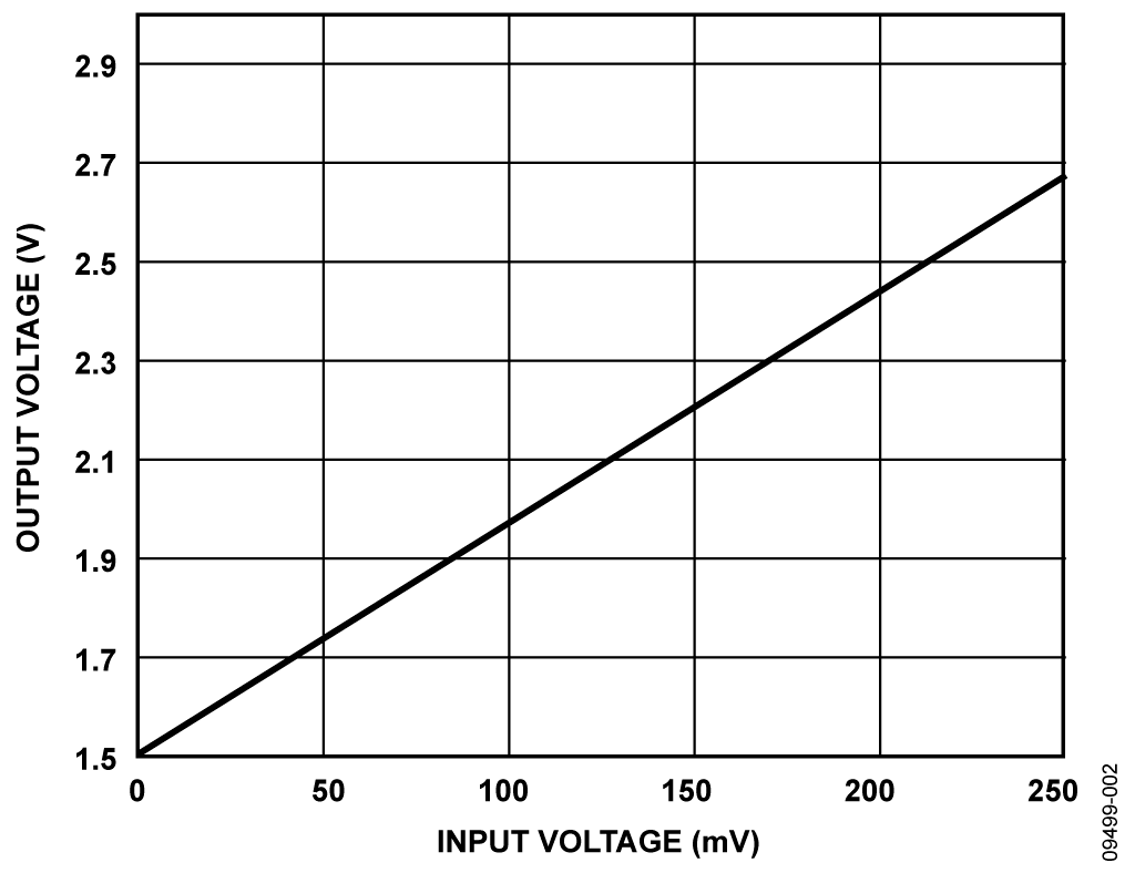
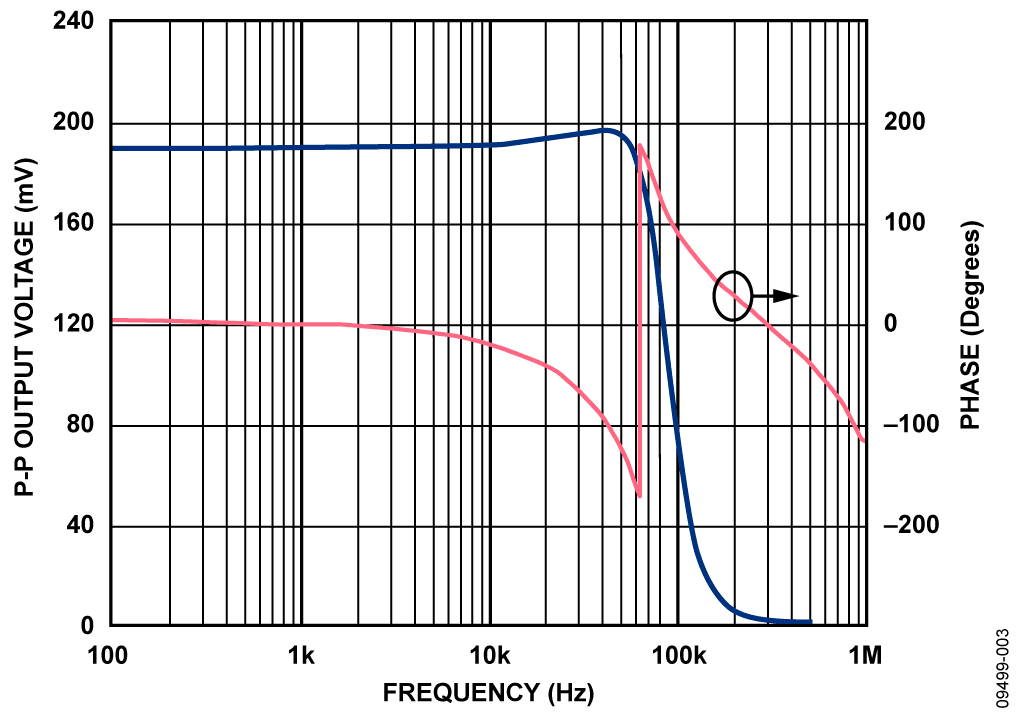
Figure 3 shows the output voltage with no dc offset voltage vs. the input frequency. The input signal voltage is 40 mV p-p, which causes an output signal of 40 × 4.6875= 190 mV p-p. Note that there is approximately 10 mV of peaking in the frequency response function, corresponding to about 0.42 dB.
The system has good noise performance, with a noise density of 2.50 μV/√Hz at 1 kHz and 1.52 μV/√Hz at 10 kHz.
A complete design support package for this circuit note can be found at www.analog.com/CN0185-DesignSupport.

Common Variations
The circuit can be used for isolated voltage monitoring and for current sensing applications where the voltage across a shunt resistor is monitored. The requirements of the input signal for the system are detailed in the AD7400A data sheet.
If the ADuM6000 is used instead of the ADuM5000, the entire circuit is rated to 5 kV.
The ADP1720 or ADP7102 linear regulator can be used as a substitute for the ADP3301, if desired.
Circuit Evaluation & Test
The circuit can be easily evaluated using a signal generator and an oscilloscope after powering on the circuit with a 6 V power supply.
Equipment Needed (Equivalents Can Be Substituted)
The following equipment is needed:
- A multifunction calibrator (dc source), Fluke 5700A
- A digital multimeter, Agilent 3458A, 8.5 digits
- A spectrum analyzer, Agilent 4396B
- A function generator, Agilent 33250A
- A power supply, 6 V
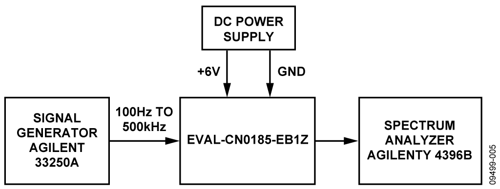
Setup and Test
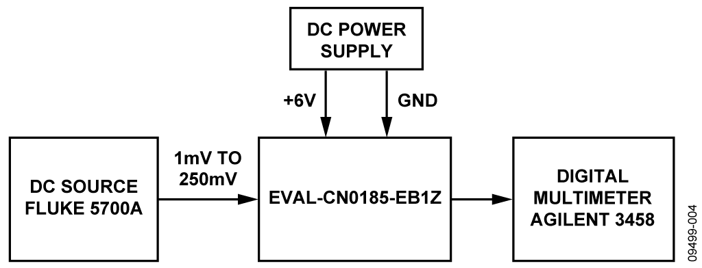
The block diagram of the linearity measurement setup is shown in Figure 4. Connect the 6 V power supply to the EVAL-CN0185-EB1Z power terminal.
The dc input voltage is generated with the Fluke 5700A, and the Agilent 3458A DVM is used to measure the output. The dc output from the Fluke 5700A is stepped, and the data recorded with a 1 mV increase from 1 mV to 250 mV.

To measure the frequency response, connect the equipment as shown in Figure 5. Set the 33250A function generator for a 40 mV peak-to-peak sine-wave output with a 0 dc offset. Then, sweep the frequency of the signal from 100 Hz to 500 kHz and record the data using the Agilent 4396B spectrum analyzer.