Introduction
Low-noise amplifiers for photodiode, piezoelectric, and other instrumentation applications typically call for circuit parameters such as extremely high input impedance, low 1/f noise, or sub-picoamp bias currents that cannot be met with available integrated products. This article discusses the requirements and challenges of designing a low-noise amplifier using discrete components, with particular emphasis on input-referred noise and offset voltage trimming.
Limitations of High Input Gain Topologies
A typical discrete amplifier, shown in Figure 1, uses a high-speed op amp preceded by a differential amplifier stage implemented with dual matched JFETs, which provide high input impedance and some initial gain. The system noise is dominated by the input stage, so a low-noise op amp is not required.
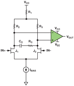
Unfortunately, stabilizing the output at low gains and high frequencies is a challenge. Stability is achieved by adding an RC compensation network, CC and RC, but the optimum values for these components change with gain, complicating the overall design. Also, the large signal response can be too slow for some applications.
The circuit shown in Figure 2 can achieve comparable noise at unity gain, without the need for compensation. The speed is primarily determined by the operational amplifier. The circuit consists of three main parts: the output op amp, the FET input buffers, and the current sources that bias the FETs.
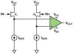
The unity-gain configuration of the input stage places a tight constraint on the op amp’s noise performance. In the circuit shown in Figure 1, the input FETs have finite gain, which reduces the noise impact of the following stage. In the unity-gain configuration, the total noise is split between the input buffers and the op amp, thus requiring a low-noise op amp.
Input Stage Current Sources
The current sources used to bias the FET input buffer can have a dramatic impact on the overall system noise if not implemented correctly. One way to minimize the bias noise contribution is to add degeneration resistors to a simple current mirror, as shown in Figure 3.
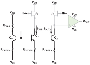
The current flowing in transistor Q0 is mirrored in transistors Q1 and Q2. The noise sources include the 1/f and shot noise of the transistors. Adding the degeneration resistors decreases the shot noise by a factor of 1 + gmRDEGEN, but has no effect on the 1/f noise. This noise source, modeled as a current between base and emitter, is not improved by adding RDEGEN. A different current source architecture is needed to reduce both noise sources simultaneously.
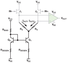
A modified current mirror is shown in Figure 4. This current source requires fewer transistors, allowing the use of a dual transistor pair instead of a quad package, and reduces both size and cost. The noise performance is vastly improved, as both shot noise and 1/f noise are canceled out. The current from transistor Q0 is mirrored to transistor Q1. This current is split at the collector using a pair of resistors, so the 1/f and shot noise will split evenly. Because the noise sources come from the same transistor, they are coherent. The output is differential, so the noise cancels out, as shown in Figure 5.
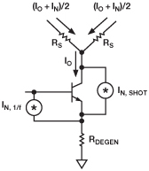
The current mirror transistors are still degenerated to improve current matching and output impedance. The current is determined by the voltage drop across RDEGEN, so transistor matching is not as important as in the undegenerated case. This allows the use of almost any matched pair, but the collector capacitance must be low to maintain stability. The differential input capacitance of the two implementations remains unchanged because the coupling between the sources of the two input devices is dominated by the low differential input impedance of the amplifier.
For the purposes of testing, the voltage reference that determines the bias current was set by a resistor connected to VCC. This leaves the circuit prone to performance issues if VCC changes. In a real implementation, a Zener, band gap, or IC voltage reference should be used instead of a resistor.
Op Amp
The op amp determines the speed, noise, output performance, and distortion of the overall amplifier, so it must be selected based on the application. Table 1 shows some typical values for suitable op amps.
Table 1. Relevant Op Amp Characteristics
| Wideband Noise (nV/√Hz) | Supply Current (mA per amplifier) | 3-dB Bandwidth (MHz @ G = 1) | Supply Voltage (V) | |
| ADA4897 | 1.0 | 3 | 230 | ±1.5 to ±5 |
| ADA4898 | 0.9 | 8 | 65 | ±5 to ±18 |
The ADA4897 is a good candidate for the low-noise performance necessitated by most high-speed sensing applications. For high-voltage applications, the ADA4898 also performs well. Able to operate with ±18-V supplies, it maintains low noise while consuming only 8 mA of supply current. Both amplifiers result in a composite design with over 50 V/µs of slew rate.
Input FETs
The input FETs determine the input characteristics of the amplifier. The best performance requires FETs that have good matching, low noise, and low input bias current. Most importantly, these JFETs determine the input offset voltage, so they must be very well matched. In the case of the LSK389, the maximum ΔVGS is 20 mV, corresponding to a VOS of 20 mV. A technique for reducing this relatively high offset voltage will be discussed later.
Table 2. Relevant JFET Characteristics
| Wideband Noise (nV/√Hz @ f = 1 kHz) | Differential Gate-to-Source Cutoff Voltage (mV max) | Gate-to-Source Saturation Current Ratio (min) | Gate Current (pA) | |
| LSK389A | 0.9 (ID = 2 mA) | 20 | 0.90 |
N/A |
| LSK489 | 1.8 (ID = 2 mA) | 20 |
0.90 | –2 to –25 |
| 2N5564 | 2.0 (ID = 1 mA) | 5 | 0.95 | –3 |
| 2SJ109 | 1.1 (ID = 3 mA) | 20 | 0.90 | N/A |
Amplifier Performance
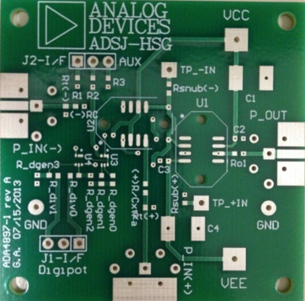
The following example uses an amplifier implemented with LSK389A nJFETs, PMP4201 transistors, and an ADA4897 op amp. The evaluation board is shown in Figure 6.
The most glaring error source of this amplifier implementation is the high input offset voltage. Largely determined by the input FET mismatch, this offset voltage can be as high as 10 mV. (The LSK389 data sheet claims mismatch as high as 20 mV, but figures this high were never seen during testing.) A gain of 100 creates a 1-V output offset, making the amplifier virtually useless. Before this amplifier can be used as a preamp, the high input offset voltage needs to be trimmed. This is done with an AD5292 digital potentiometer. Two ways to perform the offset trim based on the placement of the potentiometer are discussed here.
Input Offset Voltage
The input offset voltage for tested versions of the amplifier varied from 1 mV to 10 mV. The main cause of this offset is the mismatch of the input JFETs. The LSK389 data sheet shows that IDSS can vary by as much as 10%, affecting the VGS of the devices and introducing an offset voltage. Fortunately, the offset stems from unequal bias currents through the JFETs, so the current sources that supply these currents can be adjusted to compensate for this error. One method of achieving zero offset voltage is shown in Figure 7.
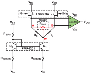
A digital potentiometer such as the AD5141 or AD5292 can be used to adjust the current through the input devices. Table 3 shows key characteristics for these devices, which consist of a three-terminal potentiometer controlled through an SPI interface to accurately position the wiper for precise resistance control.
Table 3. Digital Potentiometer Specifications
| Supply Voltage (V) | Nominal Resistance (kΩ) | Resistor Tolerance (%) | Resolution (bits) | Operating Temperature (°C) | |
| AD5141 | ±2.5 | 10, 100 | 8 | 8 | –40 to +125 |
| AD5292 | ±16 | 20, 50, 100 | 1 | 10 | –40 to +105 |
Unfortunately these digital potentiometers have high parasitic capacitances at their terminals (up to 85 pF), which cause stability issues and ringing at high frequencies. Figure 8 shows the step response of the amplifier with and without this potentiometer.
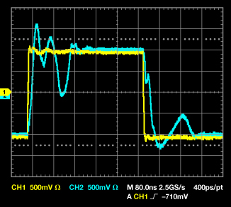
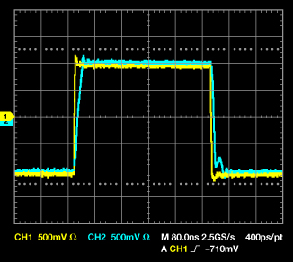
The 85 pF of parasitic capacitance is connected between the source of the input FETs and ground, causing significant ringing and instability at high frequencies. An alternative biasing setup that reduces input offset voltage while maintaining low noise and stability at high frequencies is shown in Figure 9.
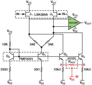
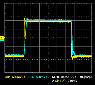
In both of the above biasing methods, the digital potentiometer is used to adjust the current through each FET until their gate-to-source voltages are matched and the input offset voltage is minimized. However, the biasing scheme of Figure 9 ensures that the high parasitic capacitance of the potentiometer does not cause high-frequency instability and ringing. It works by combining the two different current mirror configurations of Figure 3 and Figure 4. The Q0/Q1 current mirror provides the majority of the current to the FETs by splitting its collector current, introducing almost no noise from the biasing transistors. Q0/Q2/Q3 form a more traditional, yet noisier, current mirror. These are degenerated so that they only source 1% to 2% of the total FET bias current (about 30 µA). This is not enough to introduce significant noise, but allows enough adjustment to easily trim a 10-mV offset. More importantly, it ensures that the parasitic capacitance of the potentiometer does not affect the output. Thus, the noise remains low thanks to the RS splitters, the offset can be trimmed reliably based on the degeneration of Q2/Q3, and any potentiometer parasitics have no effect on the output. Figure 10 shows the step response for the mirror trimmed version.
Digital potentiometers provide an easy way to trim the offset voltage, allowing for a wide range of operating temperatures and voltages under which the offset can be minimized. The AD5292 includes a 20-times programmable memory that allows the wiper position to be stored permanently after adjusting the offset voltage. This circuit implementation used an AD5292 evaluation board to connect the offset trimming potentiometer off-board. For more compact designs, the digital potentiometer could be included on board and programmed using its on-chip serial interface pins.
Using this method, the input offset voltage was successfully reduced to a few microvolts for the LSK389/ADA4897 amplifier using an AD5292 20 kΩ potentiometer.
Offset Drift
The offset voltage temperature coefficient, or the rate at which the input offset voltage increases with increasing temperature, is about 4 µV/°C for the untrimmed amplifier. The addition of the AD5292 increases this to about 25 µV/°C. These results are shown in Figure 11.
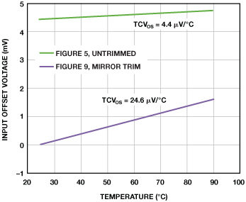
Despite the large change in drift, the dynamic range of the amplifier is improved considerably. Consider an untrimmed amplifier with 5 mV of offset at a gain of 100 and temperature of 85°C. This creates an output offset of
VOUT = (VOS + TCVOS × T) × G = (5 mV + 4 µV/°C × 85°C) × 100 = 534 mV.
If the offset was trimmed to 5 µV at the same operating conditions, the output offset would be
VOUT = (VOS + TCVOS × T) × G = (5 µV + 25 µV/°C × 85°C) × 100 = 213 mV,
thus improving dynamic range by more than 300 mV. This also enables field calibration and system level drift calibration and trim techniques that can further improve accuracy.
Noise
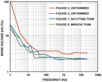
Figure 12 shows the noise density of various amplifier config-urations. This amplifier achieves a wideband noise density of 2 nV/√Hz with an 8-mA supply current, an improvement over existing integrated products. The untrimmed 1/f noise is 4 nV/√Hz at 10 Hz, and 16 nV/√Hz at 1 Hz. Note that both the 1/f and wideband noise are 1.5 to 2 times higher for the conventional current mirror (red curve), and that the overall noise remains virtually unchanged with trimming, as shown in the three other curves.
Small Signal Transfer Function
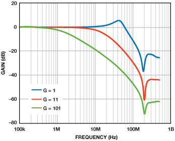
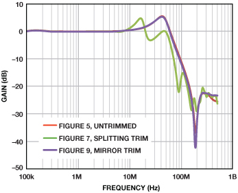
Figure 13 and Figure 14 show the frequency response for various gains and trim settings. Note that the RS trimmed amplifier is unstable and that the frequency response is the same between the untrimmed and mirror-trimmed versions.
Input Bias Current
Input bias currents were measured using a gain configuration and sense resistor. Table 4 shows typical ranges for various parts, voltages, and temperatures.
Table 4. Input Bias Current Values
| ADA4897 (25°C) | ADA4897 (125°C) | ADA4898 (±5 V) | ADA4898 (±15 V) | |
| Input Bias Current (pA) | <1 | 4000–10,000 | <1 | 15–50 |
Conclusion
With the growing number of applications that require specialized op amps with high input impedance, low noise, and minimal offset voltage, it becomes increasingly important to be able to design an application-specific circuit using discrete parts. This article described a high-speed, low-noise amplifier with adjustable input offset voltage using only four discrete parts. The design considerations for each stage were discussed, with particular emphasis on the noise performance of the amplifier and the various ways to cancel shot and 1/f noise. Using the ADA4897 op amp and LSK389 JFETs, a unity-gain capable amplifier with 2-nV/√Hz input-referred noise and only 8 mA of supply current was designed and tested. The high input offset voltage, in the range of 10 mV, was digitally trimmed using the AD5292 digital potentiometer. Alternative parts were discussed, in order to suit different applications and environments.

