Quantic X-Microwave

Analog Devices RF and microwave components are available as drop-in X-MWblocks®
from Quantic X-Microwave.

Get the X-MWblock® drop-in module for this part.

ADM7150

RECOMMENDED FOR NEW DESIGNS

800 mA, Ultra Low Noise/High PSRR LDO

Part Models
18
1ku List Price
Starting From $3.89
Viewing:

Part Details

  • Input voltage range: 4.5 V to 16 V
  • Maximum output current: 800 mA
  • Low Noise:
    1.0 μVRMS Total Integrated Noise from 100 Hz to 100 KHz
    1.6 μVRMS Total Integrated Noise from 10 Hz to 100 KHz
  • Noise Spectral Density <1.7nV√Hz above 10 KHz
  • PSRR of >90 dB from 1 KHz to 100 KHz, >60dB @ 1 MHz, VOUT = 5V
  • Dropout voltage: 600 mV @ VOUT = 5 V/800 mA load
  • Initial accuracy: ±1%
  • Accuracy over line, load, and temperature: ±2%
  • Quiescent Current, IGND = 4.3 mA @ No Load
  • Low shutdown current: 0.1 μA
  • Stable with a 10 μF ceramic output capacitor
  • Fixed output voltage options: 1.8 V, 2.8 V, 3.0 V, 3.3 V and 5.0 V
    (16 outputs between 1.5 V and 5.0 V are available)
  • 8-lead LFCSP package and SOIC package

ADM7150
800 mA, Ultra Low Noise/High PSRR LDO
ADM7150 Functional Block Diagram ADM7150 Pin Diagram
Add to myAnalog

Add product to the Products section of myAnalog (to receive notifications), to an existing project or to a new project.

Create New Project
Ask a Question

Documentation

Learn More
Add to myAnalog

Add product to the Products section of myAnalog (to receive notifications), to an existing project or to a new project.

Create New Project

Hardware Ecosystem

Parts Product Life Cycle Description
ADM7151 RECOMMENDED FOR NEW DESIGNS 800 mA Ultralow Noise, High PSRR, RF Linear Regulator
Modal heading
Add to myAnalog

Add product to the Products section of myAnalog (to receive notifications), to an existing project or to a new project.

Create New Project

Tools & Simulations

LTspice 1


Models for the following parts are available in LTspice:

  • ADM7150-1.8
  • ADM7150-2.8
  • ADM7150-3.0
  • ADM7150-3.3
  • ADM7150-4.5
  • ADM7150-4.8
  • ADM7150-5.0

ADI Linear Regulator Design Tool and Parametric Search

Microsoft Excel download tool from ADIsimPower to generate a power supply design complete with a schematic, bill of materials, and performance specifications.

Open Tool
LTspice

LTspice® is a powerful, fast and free simulation software, schematic capture and waveform viewer with enhancements and models for improving the simulation of analog circuits.


Evaluation Kits

eval board
EVAL-ADM7150

ADM7150 and ADM7151 Evaluation Board
Product Details

The ADM7150CP-EVALZ and ADM7151CP-04-EVALZ evaluation boards are used to demonstrate the functionality of the ADM7150 and ADM7151 linear regulators, respectively.

Simple device measurements, such as line and load regulation, dropout, and ground current, can be demonstrated with just a single voltage source, a voltmeter, an ammeter, and load resistors.


For more details about the linear regulators, refer to the ADM7150 and ADM7151 data sheets.


Note:ADM7151 is adjustable and requires two resistors to set the output voltage

eval board
AD-PAARRAY3552R-SL

RF Front-end GaN Power Amplifier Biasing, Protection, and Control Reference Design

Features and Benefits

  • Designed to cover full Tx signal chains with integrated MCU and user-friendly GUI for faster and easier integration
  • Supports fault event protection - overvoltage (OV), overcurrent (OC), and overtemperature (OT)
  • Supports ultrafast sub-µs GaN gate voltage switching ~ (<1 µs)
  • Supports ultrafast (<10 µs) fault event protection from detection up to GaN gate pinch-off
  • Wide range of gate bias voltages from -10 V to +10 V
  • Configurable power-up and power-down sequence

Product Details

The AD-PAARRAY3552R-SL reference design provides control, protection, and proper biasing sequence for GaN power amplifier (PA) arrays. The design incorporates the AD3553R high-speed, dual-channel, 16-bit DAC to support the ultrafast sub-µs voltage settling time of GaN gates.

Key fault events, including overvoltage, overcurrent, and overtemperature, are effectively managed by the LTC7000, a static switch driver responsible for system fault protection.

The on-board MAX32666 ultralow-power ARM® Cortex®-M4 microprocessor provides essential debug and programming features for a comprehensive software development experience with the system. The system's firmware is built on ADI's open-source no-OS framework and includes a user-friendly graphical interface (GUI) for evaluation. Updates are easily applied through an SWD UART bootloader, streamlining prototyping.

The system can be powered by an external +48 V supply, requiring high current capabilities.

APPLICATIONS

  • 5G massive MIMOs
  • Macro base stations
Specifications
Fault Events
Fault Default Limit
Overvoltage +55 V
Overcurrent 3.5 A
Overtemperature 75°C
Output Ports
Port Name No. of ports
GaN gate ports 6
+48 V Gan drain ports 4
+5 V ports 5
Enable ports 2
Power Supply
External +48 V DC at 5 A
Operating Conditions
Temperature Range 45°C to +75°C

eval board
AD-FMCOMMS11-EBZ

Direct RF to Baseband Transmit Radio

Features and Benefits

  • TX
    • 16-bit 12GSPS RFDAC
    • JESD204B Interface
      • 8 lanes up to 12.5Gbps
    • 1x/2x/4x/6x/8x/12x/16x/24x/32x Interpolation
    • 64-bit NCO at max rate
    • Analog Modes of Operation:
      • Normal Mode: 6GSPS DAC rate
        • Synthesis up to 2.5GHz (1st Nyquist)
      • Mix Mode: 6GSPS DAC rate
        • Synthesis in 2nd & 3rd Nyquist zones
      • 2X Normal Mode: 12GSPS DAC rate
        • Synthesis up to 6GHz (1st Nyquist)
      • Excellent dynamic performance
  • RX
    • 3.2GHz full power bandwidth at 2.5GSPS
      • Noise Density = -149.5dBFs/Hz, ENOB = 9.5 bits
      • SFDR = 77 dBc at 1GHz Ain (2.5Gsps)
      • SFDR = 77dBc at 1.8GHz Ain (2.5Gsps)
    • +/-0.3 LSB DNL, +/-1.0 LSB INL
    • Dual supplies : 1.3V and 2.5V
    • 8 or 6 Lane JESD204B Outputs
    • Programmable clipping threshold for Fast Detect output
    • Two Integrated wide band digital down converters (DDC) per channel
      • 10-bit complex NCO
      • 2 cascaded half band filters (dec/8, dec/16)
    • Timestamp for synchronous processing alignment
      • SYSREF Setup/Hold detector
    • Programmable Interrupt (IRQ) event monitor

Product Details

The AD-FMComms11-EBZ board is a system platform board for communication infrastructure applications that demonstrates the Direct to RF (DRF) transmitter and observation receiver architecture. Using high sample rate RFDAC(s) and RFADC(s), a number of components in previous generation transmitters can be eliminated, such as mixers, modulators, IF amplifiers and filters. The objective being to bring the ADC or DAC as close to the antenna as possible, leading to possibly more cost effective and efficient communications solution.

It is composed of multi-GSPS RF ADC and DAC, AD9625 and AD9162 respectively. The transmit path contains a balun, low pass filter, gain block and variable attenuation to produce an output appropriate for a power amplifier module. Along the observation path, the PA output is coupled back into the board through a variable attenuator, a balun and finally the ADC. Clock management is taken care of on board; all the necessary clocks are generated from a reference. Power management is present as well.

eval board
AD-FMCOMMS6-EBZ

AD-FMCOMMS6-EBZ Evaluation Board

Features and Benefits

  • Reduces receiver complexity and the number of stages needed, increasing performance and reducing power consumption 
  • Avoids image rejection issues and unwanted mixing 

Product Details

The AD-FMCOMMS6-EBZ eval board is a 400MHz to 4.4GHz receiver based on the AD9652 dual 16bit analog to digital converter, the ADL5566 High Dynamic Range RF/IF Dual Differential Amplifier and the ADL5380 quadrature demodulator.

This is an I and Q demodulation approach to direct convert (also known as a homodyne or zero IF) receiver architecture. Direct conversion radios perform just one frequency translation compared to a super-heterodyne receiver that can perform several frequency translations. One frequency translation is advantageous because it:

  • Reduces receiver complexity and the number of stages needed, increasing performance and reducing power consumption
  • Avoids image rejection issues and unwanted mixing


This topology will provide image rejection and early implementation of the differential signal environment. There is an amplification stage to maintain the full-scale input to the ACD. The local oscillator and ADC clock are on board and share the same reference signal prevent smearing. The form factor is VITA57 compliant and all of the DC power is routed from the data capture board through an FMC connector. This evaluation board demonstrates a high performance receiver signal chain aimed at military and commercial radar using “commercial off the shelf” (COTS) components. The overall circuit has a bandwidth of 220MHz with a pass band flatness of +/_ 1.0 dB. The SNR and SFDR measured at an IF of 145MHz are 64dB and 75dBc, respectively.


eval board
AD-ACEVSE22KWZ-KIT

AD-ACEVSE22KWZ-KIT

Features and Benefits

  • Metrology subsystem plus selected other features of a level 2, 7kW to 22kW electric vehicle supply equipment (EVSE)
  • Full-featured board for ADE9112, ADE9113, and ADE9178
  • Rated up to three phase, 240V RMS line to neutral voltage
  • Rated up to 32A current measurement with on-board shunts
  • Supports up to 22kW combined power transfer to load
  • Features MAX32672 low power, secure microcontroller
  • Supports LCD display for energy and state updates
  • Supports MODBUS™ protocol over RS-485 communication interface
  • Supports Protobuf™ messages to communicate with EVerest open source software (OSS)
  • IEC61851-compatible state machine implementation

Product Details

The AD-ACEVSE22KWZ-KIT is a reference design for the metrology subsystem plus selected other features of a level 2, 7 kW to 22 kW AC electric vehicle supply equipment (EVSE). It includes the ADE9113 isolated Σ-Δ analog-to-digital converter (ADC) coupled with the ADE9178 metrology DSP to accurately measure energy delivered to an electric vehicle (EV). It includes the MAX32672 ultralow- power ARM® Cortex®-M4 processor, a cost-effective, highly integrated, and highly reliable 32-bit microcontroller to accumulate energy measurements and securely send it to a host for display. A charge control state machine is run on the microcontroller to transition through different charge states when a charging plug is inserted into an electric vehicle. The kit includes a flexible printed circuit (FPC) connector and LCD to read the energy measurements and state transitions during a charging cycle. The power input/output, control pilot (CP), and proximity pilot (PP) signals are exposed on connectors at the edge of the board. The energy delivered to the EV is measured as a voltage drop across shunts and a resistor ladder network, which makes it easy to set up the boards in the field.

EVAL-ADM7150
ADM7150 and ADM7151 Evaluation Board
EVAL-ADM7150-7151
AD-PAARRAY3552R-SL
RF Front-end GaN Power Amplifier Biasing, Protection, and Control Reference Design
AD-PAARRAY3552R-SL Block Diagram AD-PAARRAY3552R-SL Board Photo Angle View AD-PAARRAY3552R-SL Board Photo Top View AD-PAARRAY3552R-SL Board Photo Bottom View
AD-FMCOMMS11-EBZ
Direct RF to Baseband Transmit Radio
AD-FMCOMMS11-EBZ Block Diagram AD-FMCOMMS11-EBZ Evaluation Board AD-FMCOMMS11-EBZ Evaluation Board - Top View AD-FMCOMMS11-EBZ Evaluation Board - Bottom View
AD-FMCOMMS6-EBZ
AD-FMCOMMS6-EBZ Evaluation Board
eval-image-unavailable
AD-ACEVSE22KWZ-KIT
AD-ACEVSE22KWZ-KIT
AD ACEVSE22KWZ-KIT Board Photo Angle View AD ACEVSE22KWZ-KIT Board Photo Top View AD ACEVSE22KWZ-KIT Board Photo Bottom View

Reference Designs

Figure 1. CN0511 Functional Block Diagram
CN0511 Circuits from the lab

DC to 5.5 GHz Signal Generator with +/-0.5 dB Calibrated Output Power

Features and Benefits

  • DC to 5.5 GHz Single Tone Generator
  • +/- 0.5 dB  Wideband Amplitude Calibration from 0 dBm to -40 dBm
  • 48-Bit Frequency Tuning Resolution (~43 uHz)
  • Onboard VCXO for Quick Bring Up
  • Compatible with Raspberry Pi 3B+, 4, Zero W, Zero 2W
Isolated and Nonisolated RS-485 Transceiver Simplified Schematic
CN0507 Circuits from the lab

A Complete Two-Port Vector Network Analyzer  

Features and Benefits

  • Complete 2-Port Vector Network Analyzer
  • Frequency range from 1.7 GHz to 3.4 GHz
  • Zero-IF System Architecture
CN0565 01 new
CN0565 Circuits from the lab

Electrical Impedance Tomography Measurement System

Features and Benefits

  • Up to 24 Input Electrodes, Software Selectable 
  • 2-wire or 4-wire Electrode Configuration Supported
  • Real and Imaginary Measurements up to 200 kHz
  • Open Source Image Recreation Algorithms
  • Isolated Power and Digital Domains from the Host
  • Arduino Form Factor Compatible
Figure 1. Simplified Block Diagram of EVAL-CN0534-EBZ
CN0534 Circuits from the lab

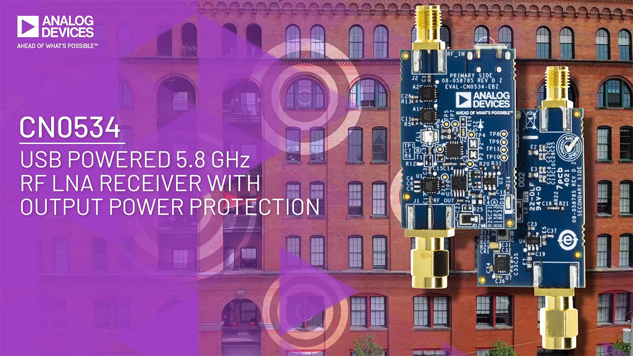
USB Powered 5.8 GHz RF LNA Receiver with Output Power Protection

Features and Benefits

  • 23.5 dB Gain
  • 5.8 GHz Optimized LNA
  • ISM Band Operation
  • USB Powered

Part Used


Design & Integration Tools


Videos

  • lazy blur
    VIDEO · 2022-01-24 01:01
    CN0534: USB Powered 5.8 GHz RF LNA w/ Output Power Protection
Figure 1. CN0521 Simplified Block Diagram
CN0521 Circuits from the lab

USB-Powered, 2.4 GHz RF Low Noise Amplifier Receiver with Overpower Protection Circuit

Features and Benefits

  • +26 dB of Rx Signal Gain
  • 50 ohm Input and Output Impedance
  • Overvoltage Input Protection
  • SMA Input and Output Connectors
  • USB Powered
Figure 1. CN0566 Simplified Block Diagram
CN0566 Circuits from the lab

Phased Array (Phaser) Development Platform

Features and Benefits

  • 10 GHz to 10.5 GHZ Beamsteering Platform
  • 360 degree Phase Shift w/ 2.8 Degree Resolution
  • 31 dB Amplitude Tuning Range w/ 0.5 dB Resolution.
  • 8-Element Linear Array Antenna
  • Digitized with PlutoSDR
  • Runs directly on a Raspberry Pi
Figure 1. CN0523 Simplified Block Diagram
CN0523 Circuits from the lab

USB-Powered, 5.8 GHz RF Power Amplifier with Overtemperature Management

Features and Benefits

  • 5.8 GHz RF Power Amplifier
  • 24 dB of Gain
  • 50 Ohm matched SMA Input and Output Connectors
  • Over Temperature Monitoring
  • USB Powered
Figure 1. CN0518 Simplified Block Diagram
CN0518 Circuits from the lab

USB-Powered, 915 MHz RF Low Noise Amplifier Receiver with Overpower Protection Circuit

Features and Benefits

  • +25 dB of Rx Signal Gain
  • 50 ohm Input and Output Impedance
  • Overvoltage Input Protection
  • SMA Input and Output Connectors
  • USB Powered
Block Diagram of the Translation Loop Synthesizer
CN0369 Circuits from the lab

Translation Phase Locked Loop Synthesizer with Low Phase Noise

Features and Benefits

  • Translation Loop Synthesizer 
  • 5GHz to 5.4GHz RF Output 
  • Low Phase Noise
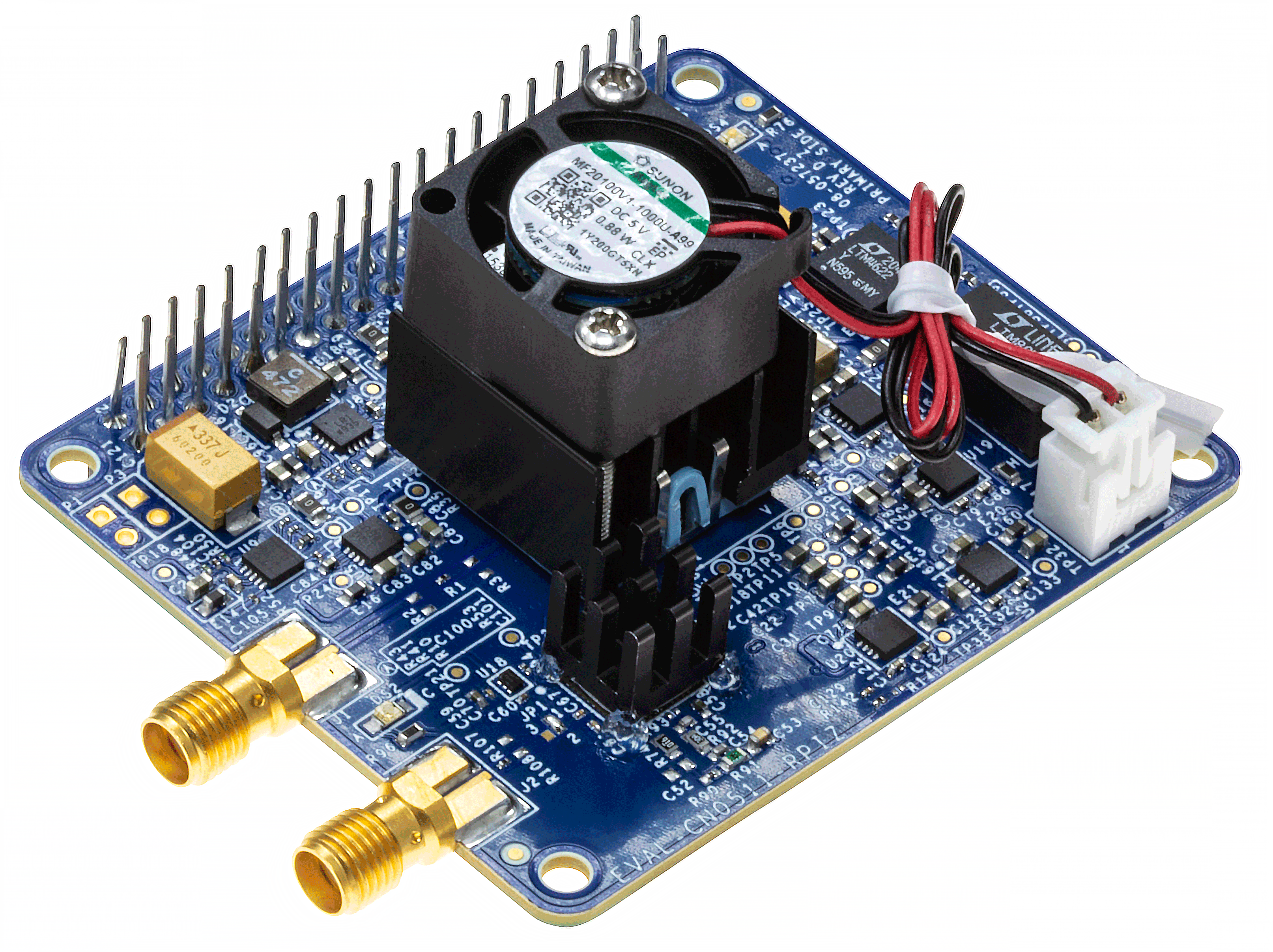
CN0511
DC to 5.5 GHz Signal Generator with +/-0.5 dB Calibrated Output Power
Figure 1. CN0511 Functional Block Diagram
EVAL-CN0511-RPIZ Evaluation Board
EVAL-CN0511-RPIZ Evaluation Board - Top View
EVAL-CN0511-RPIZ Evaluation Board - Bottom View
CN0507
A Complete Two-Port Vector Network Analyzer  
Isolated and Nonisolated RS-485 Transceiver Simplified Schematic
EVAL-CN0507-ARDZ Evaluation Board
EVAL-CN0507-ARDZ Evaluation Board - Top View
EVAL-CN0507-ARDZ Evaluation Board - Bottom View
CN0565
Electrical Impedance Tomography Measurement System
CN0565 01 new
EVAL-CN0565-ARDZ
EVAL-CN0565-ARDZ - Top View
EVAL-CN0565-ARDZ - Bottom View
EVAL-CN0565-ARDZ with Test Board
CN0534
USB Powered 5.8 GHz RF LNA Receiver with Output Power Protection
Figure 1. Simplified Block Diagram of EVAL-CN0534-EBZ
EVAL-CN0534-EBZ - Angle View
EVAL-CN0534-EBZ - Top View
EVAL-CN0534-EBZ - Bottom View
CN0521
USB-Powered, 2.4 GHz RF Low Noise Amplifier Receiver with Overpower Protection Circuit
Figure 1. CN0521 Simplified Block Diagram
EVAL-CN0521-EBZ
EVAL-CN0521-EBZ - Top View
EVAL-CN0521-EBZ - Bottom View
CN0566
Phased Array (Phaser) Development Platform
Figure 1. CN0566 Simplified Block Diagram
EVAL-CN0566-RPIZ Phased Array Development Kit
EVAL-CN0566-RPIZ KIT - Angle View
CN0523
USB-Powered, 5.8 GHz RF Power Amplifier with Overtemperature Management
Figure 1. CN0523 Simplified Block Diagram
CN0518
USB-Powered, 915 MHz RF Low Noise Amplifier Receiver with Overpower Protection Circuit
Figure 1. CN0518 Simplified Block Diagram
EVAL-CN0518-EBZ
EVAL-CN0518-EBZ - Top View
EVAL-CN0518-EBZ - Bottom View
CN0369
Translation Phase Locked Loop Synthesizer with Low Phase Noise
Block Diagram of the Translation Loop Synthesizer
EVAL-CN0369-SDPZ PCB Photo

Latest Discussions

Recently Viewed